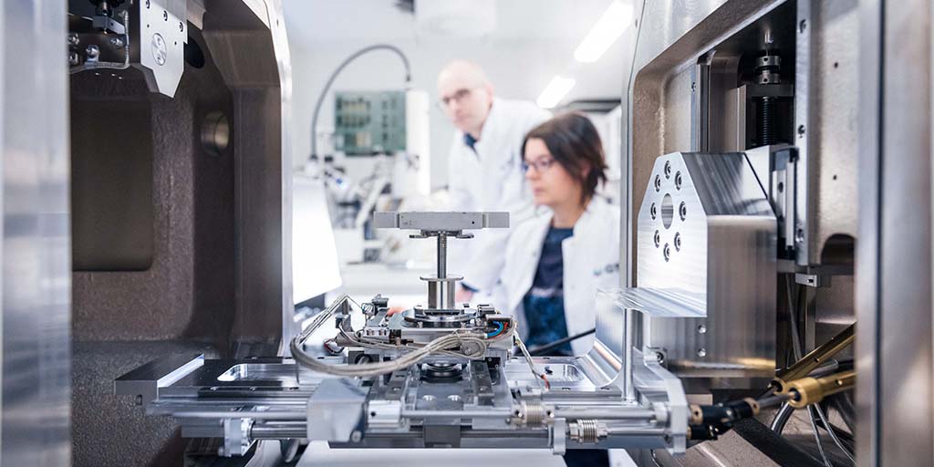
Electron optics and microanalysis
GTK has a long history in microanalysis and electron optics. Our first microanalyser was acquired for research purposes as early as 1965. Electron optical analysis is the basic tool of mineralogical surveying. GTK has four scanning electron microscopes (SEMs): two in Espoo, two in Outokumpu. The Research Laboratory in Espoo also has a microanalyser.

Scanning electron microscopy
GTK has four scanning electron microscopes (SEMs): two in Espoo, two in Outokumpu (see table). Both locations feature one “traditional” SEM with tungsten filaments, and one more modern SEM using field emission (FE-SEM). The traditional SEM can produce images at 10,000X magnification in optimal conditions, and it can produce images of particles with a size of less than one micron. The FE-SEM can reach a magnification of several hundred thousands, and it can produce nanometre-scale images.
All GTK’s SEMs are connected to an energy-dispersive X-ray spectrometer (EDS/EDX), which means that in addition to imaging, they can be used to analyse the chemical element composition of samples. The equipment enables us to analyse a variety of mineral-based materials and other inorganic materials.
Some SEMs have an LV feature, which enables samples to be analysed in a pre-set low vacuum. This means samples do not need to be separately prepared for analysis. However, in low vacuum conditions, the analysis accuracy is not as good as in high vacuum conditions.
The results of EDS analysis are semi-quantitative. The measuring accuracy of chemical element contents varies depending on sample but is usually around 0.3–0.5 weight percent (wt%). Samples with a grain size less than 1–3 μm cannot be analysed reliably. Nor is exact identification of mineral phases from an EDS spectrum always possible. In addition, phases with similar or identical chemical composition cannot be distinguished from each other.
EDS systems are operated with a set of software that enables analyses to be conducted largely automatically. Point or line analyses can be conducted on samples, their modal mineralogy can be analysed, and automatic searches related to them can be performed. In addition, dispersal maps on chemical elements can be prepared, and data can be produced on grain size distribution and mineral associations and liberations for use in mineral processing.
GTK’s SEM and EDS equipment
| Location | ID | SEM | EDS | Software |
|---|---|---|---|---|
| Espoo | LV-SEM-EDS | Hitachi SU3900 | Oxford Instruments X-Max N 20 mm2 | INCA |
| Espoo | FE-SEM-EDS | JEOL JSM 7100F Schottky | Oxford Instruments X-Max SDD 80 mm2 | INCA, Aztec |
| Outokumpu | SEM-MLA | FEI Quanta 600 | Edax Genesis EDX (2 kpl) | MLA |
| Outokumpu | FE-SEM-MLA | FEI Quanta 650 | Bruker XFlash EDX (2 kpl) | MLA, QEMSCAN, AMICS |
Microanalysis
Microanalysis by means of an electron probe microanalyzer (EPMA) is an important mineralogical quantitative analysis method and often needed to supplement SEM and EDS as well as LA-SC-HR-ICP-MS analyses, for example. The GTK Research Laboratory in Espoo has two EPMAs that enable us to do quantitative analysis of nearly all elements on the periodic table (Be–U). The Cameca SX100 equipment features five wavelength-dispersive spectrometers (WDS) that are used in routine quantitative analysis. The state-of-the-art JEOL JXA-iHP200F Hyperprobe, also equipped with five WDS detectors, is a field emission microanalyzer (FE-EPMA) enabling high precision quantitative analysis even in sub-micron range and high accuracy quantitative element mapping.
In routine analyses, the chemical-element-specific detection limits are around 0.01%, or as low as 10 ppm if a long measurement time is used in trace element analysis. The chemical elements to be analysed are selected beforehand. Both microanalyzer also feature an EDS detector for qualitative analysis, as well as BSE, SEI and the CAMECA SX100 also a CL-detector for imaging.
Point, profile, or grid analysis can be conducted with both microanalyzer. The smallest area in routine analysis is an area of around 1–2 microns in diameter. Usually, mineral structures and other targets to be analysed must be identified with optical microscopy or SEM beforehand.
